

Semiconductor Precision Manufacturing | ZHD Precision
Semiconductor Product Development & Precision Manufacturing
Accelerate innovation for semiconductor equipment, wafer processing systems and microelectronic component platforms with ZHD Precision. We reduce engineering risks and shorten project cycles via certified ultra-precision prototyping, micro machining and large-scale mass production solutions.
- PARTSemiconductor-grade ultra-precision components
- DFMDFM feedback within 24 hours
- ENGInstant quotation & 24/7 professional engineering support
- QCFull-process cleanroom quality inspection
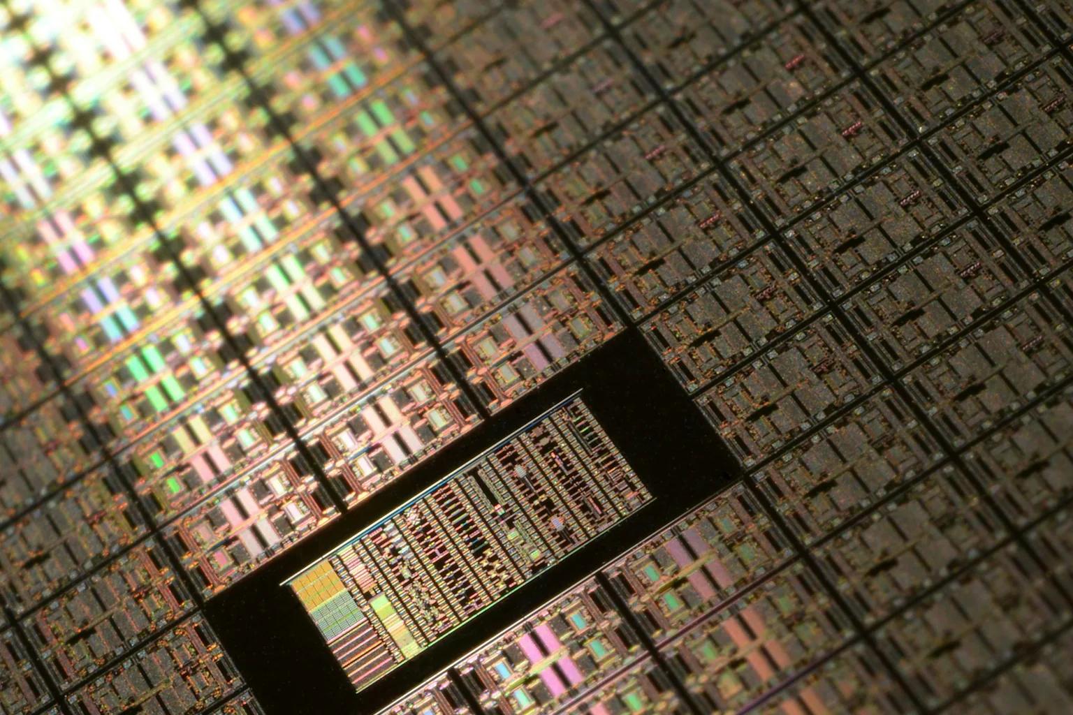
Industry reference: patterned semiconductor wafer
Treat contamination behavior as part of the mechanical specification.
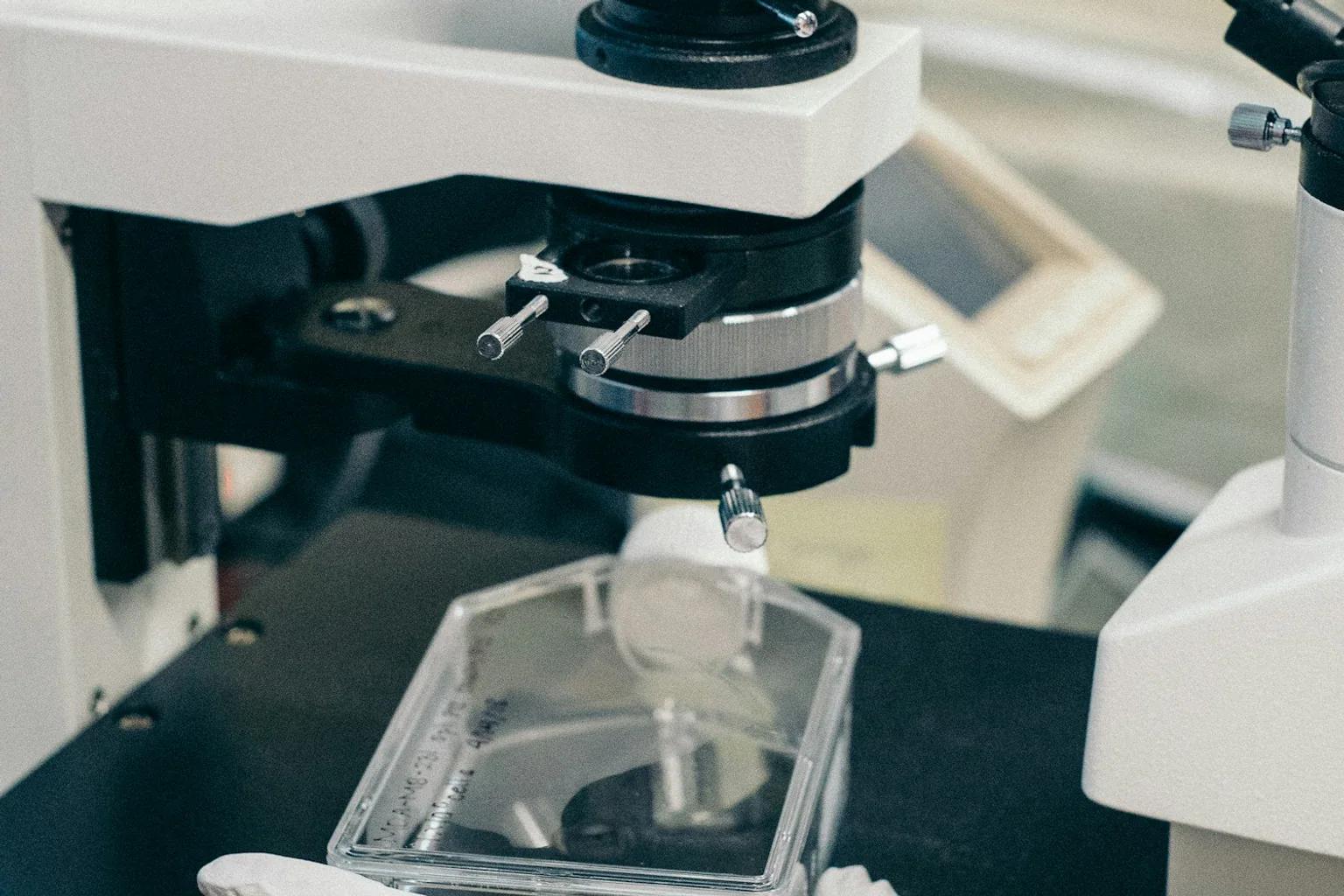
Semiconductor equipment parts must connect micro-dimensional control with particle prevention, low-outgassing materials, vacuum surfaces and clean packaging.
- 01
Material purity
- 02
Micro machining
- 03
Surface control
- 04
Clean inspection
- 05
Protected packing
Cleanliness, vacuum and ESD control
We support prototype, validation, and production programs for organizations developing demanding industry equipment and components.
Requirements Review
Applicable quality, traceability, and documentation requirements are reviewed before production.
Machining tolerance
±0.005mm
Cleanroom standard
ISO 14644-1
Release focus
Micro CTQ
Surface Finishes
Selected surface route
Semiconductor Grade High-Cleanliness Surface Finishes
We deliver standardized semiconductor-grade surface finishes processed in dust-free cleanrooms, achieving low-outgassing, anti-static, zero-particle and high-stability performance, and meeting strict ultra-clean manufacturing standards for chip and microelectronic equipment.
Traceable release packet
Quality Inspection & Compliance Documents
Complete Inspection Reports & Global Compliance
Advanced high-precision CMM & CNC VMM full inspection reports
Precision Micro-dimensional Reports (PDR)
First Article Inspection (FAI)
High-purity Material Test Reports & Cleanliness Certificates
Official Certificate of Conformance (CoC)
Full process traceability & micro-precision CTQ real-time monitoring
Quality Certifications
Authorized Certifications & Standard Compliance
Total delivered projects: 6000+
Selected compliance control
ISO 9001:2015
Professional semiconductor manufacturing quality certification, strict control over micro-dimensional accuracy, ultra-clean production consistency and full lifecycle traceability for core semiconductor equipment components.





Core Manufacturing Services
Advanced Production Technologies for Semiconductor Components

Selected manufacturing route
3/4/5 Axis Ultra-precision CNC Milling
High-precision multi-axis micro milling for wafer processing parts, vacuum chamber structures and semiconductor core fixtures. Tolerance up to ±0.005mm. Supports complex micro geometric parts, lead time as fast as 24 hours.
Material
Stainless Steel
Recommended Process
CNC Micro Machining, Sheet Metal
Core Advantages
High purity, low particle emission, excellent corrosion resistance, non-magnetic
Typical Application Parts
Vacuum chamber parts, wafer fixture bases, cleanroom structural components
Semiconductor Components We Manufacture
Full Range of Custom Semiconductor Ultra-precision Parts We manufacture diversified ultra-precision components made of high-purity metals and special engineering plastics for the semiconductor industry. All products meet micro-level ultra-tight tolerance requirements for core chip manufacturing assemblies, adopting certified low-outgassing, anti-corrosion and high-cleanliness materials, with 100% full inspection via high-precision CMM and automatic testing equipment.
Why Choose ZHD Precision
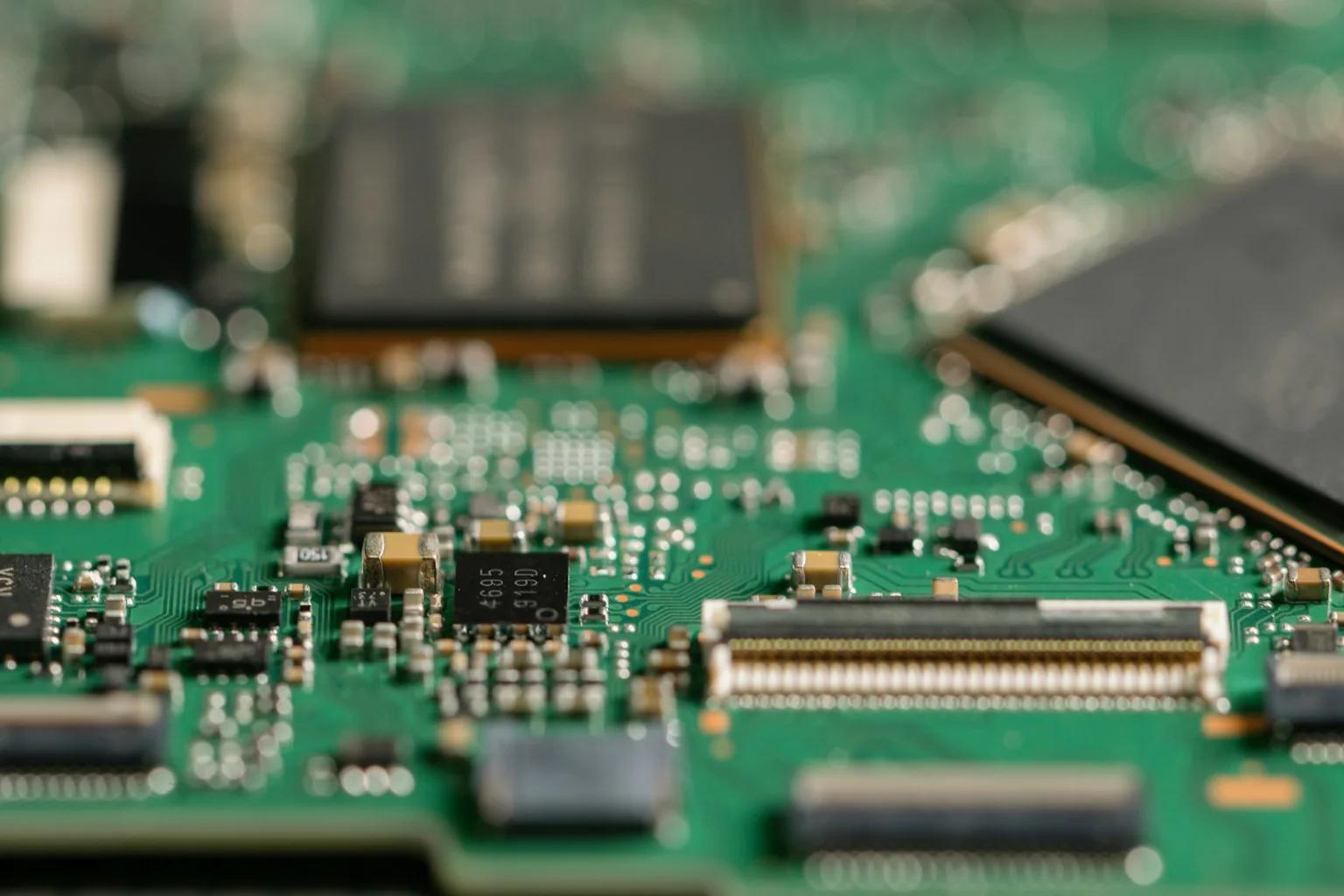
ZHD Precision has 17 years of in-depth experience in semiconductor equipment prototyping, trial production and mass manufacturing. We serve global semiconductor equipment manufacturers and microelectronics suppliers, delivering ultra-precision components that comply with the strict cleanliness and tolerance standards of the semiconductor industry. Our digital manufacturing workflow realizes seamless transition from CAD drawings to high-purity, high-precision physical parts.
Selected manufacturing control
Semiconductor-grade Standard Operation
Follows the highest semiconductor clean manufacturing specifications to ensure ultra-high precision, low particle emission and operational stability for core wafer processing and chip manufacturing systems.
Representative Applications
Representative project details can be reviewed according to application, material, process, inspection, and confidentiality requirements.
Confidential project review
Review a representative semiconductor program through its actual engineering context.
Review dimension
Application
Review dimension
Critical risk
Review dimension
Material and process
Review dimension
Inspection evidence
Review dimension
Confidentiality